What makes vertiGAN™ so great?
What makes vertiGAN™ so great?
vertiGAN™ got its name from the fundamental nature of the device structure. It is one of the world’s first commercially available devices that utilizes a vertical architecture to direct current through the device. As we will see later, the other GaN solutions use a structure that diverts the current laterally, substantially limiting the voltage and applications of the device.
| Material | Si | SiC | GaN |
|---|---|---|---|
| Critican Field (MV/cm) | 0.3 | 3.0 | 3.9 |
Table 1. Critical Fields of different semiconductor materials
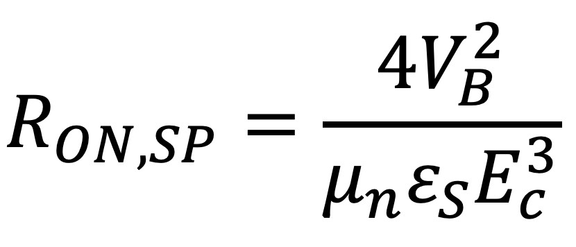
Eq 1
Many Advantages
The best way to explain the advantages of vertiGAN™ is to start with the basics. Assuming the simplest form of a device (1D-unipolar), the resistance (efficiency) of a power device is a function of the critical field of that material. The critical field is a bit complicated, but the easiest way to think about it is “the maximum electric field that can be applied to a 1D material before really bad things start to happen”. Table 1 shows the critical field of GaN vs Si and SiC (another contender against Si)
Superior Resistance
Plot 1 shows the specific on-resistance of the 3 materials vs the breakdown voltage of the device according to equation 1. GaN has a critical field that is 13x larger than Si and 1.6x larger than SiC. From Eq.1, GaN’s resistance is 1500x lower than Si and 8x lower than SiC.
Despite its clear advantage, the power electronic community has not been able to take advantage of the full power of GaN because there was no way to make the standard vertical architecture devices. On the next page, you can see how Alithia has solved that problem and is applying solutions that are >10x better than Silicon in many ways
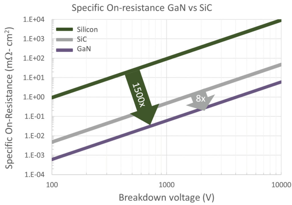
Plot 1. Specific on-resistance of different semiconductor materials vs different breakdown voltages